As the name implies SSTL is. Bandwidth for device memory.
2
The Cadence Denali High-Speed DDR PHY IP provides low latency and 4266Mbps throughput while balancing power consumption and minimizing area.

. High speed DDR memory interface design. Setting Up Your Design for Successful DDR Memory Routing. As the bandwidth requirement increases Double Data Rate DDR interface is becoming very commonly used in many types of memories such as DDR IIIIII DRAM RLDRAM III QDR IIIII SRAM etc.
This can be more complicated than you would think though when it comes to high speed memory routing. During bringup of the DDR interface the controller turns on differential DQS in the DRAM. 09162014 AR58435 - Memory Interface UltraScale IP Release Notes 03312021.
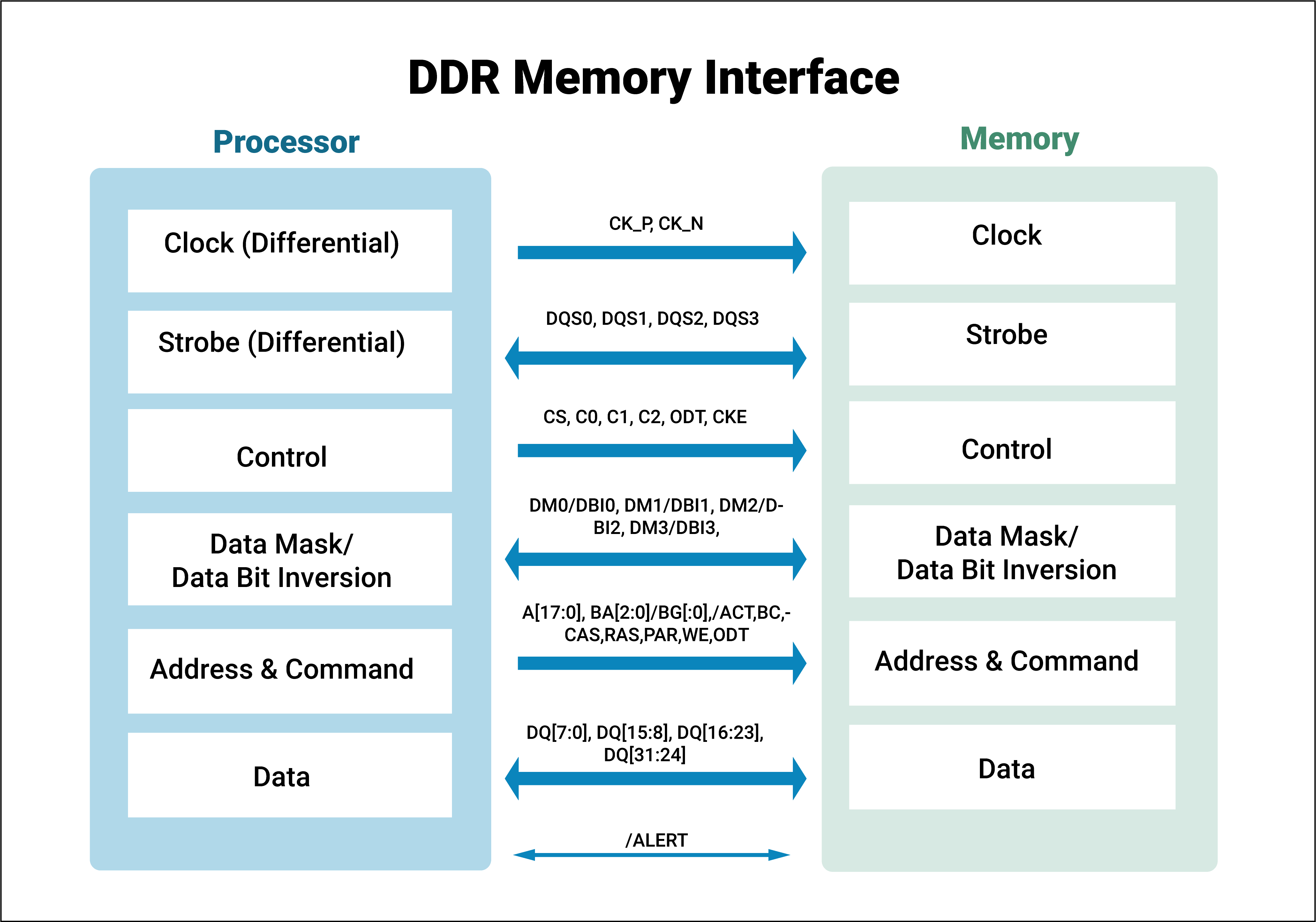
External double data rate DDR memory types are a common part of many FPGA designs. Because a DDR memory subsystem includes the controller PHY and IO it serves as a critical component of the System on Chip SoC designs used in cell phones high-definition televisions and other consumer electronic devices. As part of the overall design DDR memory controller and memory.
Since you will be dealing with high-speed circuitry you may need to consider other board materials than standard FR-4. High Speed Memory Interface Chipsets Let Server Performance Fly The demands on server performance continue to increase at a tremendous pace. DFI Group Releases Initial Version of the DFI 50 Specification for High-Speed Memory Controller and PHY Interface AUSTIN Texas May 2 2018 The DDR PHY Interface DFI Group today released version 50 of the specification for interfaces between high-speed memory controllers and physical PHY interfaces to support the requirements of future mobile.
The major feature of DDR interface compared to a single data rate SDR one is to. While measurement capability and usability are critical to speed up the verification and debug process it is equally important to choose the right probing solution and use advanced techniques to improve overall measurement accuracy. The first step in preparing to design a board with DDR memory routing on it is to plan the board layers and configuration.
The major feature of DDR interface compared to a single data rate SDR one is to use both rising and falling edges of a clock to transfer data which allow it to provide two times the. As the bandwidth requirement increases Double Data Rate DDR interface is becoming very commonly used in many types. This paper focuses on controlling synchronous dynamic random access memory SDRAM higher data transfer rates when multiple locations in internal memory array are accessed successively.
Download Citation High speed DDR memory interface design form only given. Doing so will quickly get your design all tangled up. Developed by experienced teams with industry-leading.
It is not necessary to route the ADDR bus the same length to every chip. New requirements from large in-memory databases that are powering todays cloud services and advanced analytics tools are arriving just as the impact of Moores Law is starting to slow. Ad Browse discover thousands of brands.
As the bandwidth requirement increases Double Data Rate DDR interface is becoming very commonly used in many types of memories such as DDR IIIIII DRAM RLDRAM III QDR IIIII SRAM etc. The Market Need for High Speed Memories SDRAMs have traditionally been used in personal computers PCs. Design of high speed DDR SDRAM controller with less logic utilization.
Building reliable high-speed memory interfaces target FPGA IO structures as well as intellectual property IP used within design software to allow rapid configuration of memory interfaces. The Denali High-Speed DDR PHY IP provides low latency and up to 4266Mbps throughput while balancing power consumption and minimizing area Developed by experienced teams with industry-leading. Working closely with JEDEC Rohde Schwarz provides powerful solutions for DDR compliance testing.
SSTL leverage s an active motherboard termination scheme and overcomes the signal integrity concerns with legacy LVTTL signaling. DQS needs to be the target of thematched group for each data byte regardless of whether its a single ended or differential signal. Register for our Step-by-step guide and get the right tool for advanced probing in DDR3DDR4 design.
The Cadence Denali DDR family of high-speed interface IP connects to external memories with the necessary bandwidth for applications. The need for increasing speed higher memory size and power efficiency is driving the evolution in DDR and LPDDR interface technology as defined by JEDEC. Bandwidth for device memory.
DDR Memory and the Challenges in PCB Design. Small fast-memory DDR memory. PCB Designs use DDR3 memory because of its low power high signaling speeds and large bandwidth.
Modern electronic designs such as mobiles laptops cloud computing and networking demand very high performance. A high-speed interface cell delivers 800 Mbspin data transfer rate on a 26b wide IO interface consisting of a dual-byte data field and a byte-wide command field. The Cadence Denali DDR family of high-speed interface IP connects to external memories with the necessary bandwidth for applications.
28 rows Introduction Date XTP359 - Memory Interface UltraScale Design Checklist PG150 - UltraScale Architecture FPGAs Memory IP Product Guide 08112021 PG150 - Creating a Memory Interface Design using Vivado MIG 08112021 Designing with UltraScale Memory IP. The controller is designed to interface DDR memory modules and memory ICs with low cost. DDR SDRAMs were introduced as a cost-effective path for upgrading data bandwidth to memory.
As processor core speeds exceeded 2 GHz revolutionary changes in memory speed efficiency size and costs were required to support these processor enhancements. Summary form only given. The Double Data Rate DDR memories have been a common choice of designers in all.
Lets take a look at some of the DDR routing techniques that will help you. For DDR-I memories JEDEC created and adopted a low voltage high-speed signaling standard called series stub termination logic SSTL. The DDRAM is based on 2n pre-fetch architecture that can achieve two data words per clock pulse at the IO pins for a single read or write access.
DDR SDRAM Main Controller Block Before it is operational the DDR SDRAM memory. Read customer reviews find best sellers. Double-Data Rate or DDR memory is very common in printed circuit board design today.
These techniques use IP to help gain an extra timing margin at high speed operation. The Importance of DDR Routing Techniques. Apart from processor speedperformance memories play a very critical role in overall system performance.
Design verification and debugging - Compliance testing. Due to the lack of computational resources to adequately simulate a large DDR interface designers who choose to use 3D full-wave extractions quite often segment their design into smaller pieces. This requires a high level of expertise and can be prone to errors.
The DDR SDRAM uses DDR architecture to achieve high-speed operation.

Figure 1 From Design And Implementation Of High Speed Ddr Sdram Controller On Fpga Semantic Scholar
Ddr Memory And The Challenges In Pcb Design Sierra Circuits

Ddr Phy Ip For Soc Designs Cadence Ip
How To Successfully Realize A High Speed Memory Interface In Your Design

Ddr Memory Interface Basics 2017 07 05 Signal Integrity Journal
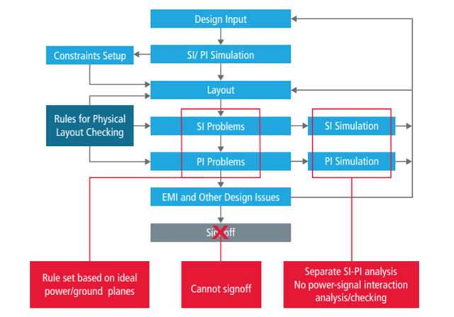
Implement Si And Pi In High Speed Memory Interfaces Signal And Power Integrity Pcb Ic Packaging Cadence Blogs Cadence Community

Pdf High Bandwidth Memory Interface Design Based On Ddr3 Sdram And Fpga Semantic Scholar
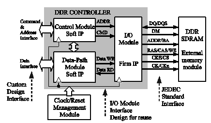
Ddr Sdram Controller Ip Designed For Reuse
0 comments
Post a Comment